Generated from a Jupyter notebook
This page is CGV/cgv_analysis.ipynb, rendered with its stored outputs.
Run it in Google Colab or
view the notebook on GitHub.
Capacitance-Voltage and Conductance-Voltage (C-V/G-V)
A C-V/G-V measurement puts a small AC signal on top of a DC bias and reads the resulting admittance. The capacitance traces how far the depletion layer under a gate moves as bias changes, so its slope gives a doping profile. The conductance traces energy lost to charge hopping in and out of interface states, so its frequency dependence gives an interface trap density. One sweep, two very different stories, because one component is reactive and the other is dissipative.
This notebook builds a MOS (metal-oxide-semiconductor) capacitor from first principles, uses its C-V curve to extract a doping profile, shows that the same algebra collapses to the classic Mott-Schottky line the moment the oxide is removed, and then uses the G-V data from the same sweep to find an interface trap density.
| Section | Question answered |
|---|---|
| 1 | What do we actually do when we sweep bias and read capacitance? |
| 2 | What is a MOS capacitor, and why does it behave like two capacitors in series? |
| 3 | What happens at the semiconductor surface as the gate bias changes? |
| 4 | Why is the semiconductor's share of the capacitance itself bias-dependent? |
| 5 | Why does measurement frequency change the shape of the curve? |
| 6 | What does the ideal C-V curve look like, feature by feature? |
| 7 | Where does the voltage axis sit - flat-band voltage and oxide charge |
| 8 | Where does inversion begin - threshold voltage |
| 9 | How do we turn C(V) into a doping profile? |
| 10 | What happens without an oxide? Schottky C-V and the Mott-Schottky line |
| 11 | What is the conductance method actually measuring? |
| 12 | How do we get the semiconductor's true parallel conductance out of what the meter reports? |
| 13 | What does the conductance peak tell us about interface traps? |
| 14 | How would you compute a C-V curve from scratch? |
| 15 | What does the space charge look like without the Boltzmann shortcut? |
| 16 | Putting it together: the full gate-voltage balance |
| 17 | Non-uniform charge, and the full trap admittance |
| 18 | What ruins a real measurement, and how do you know? |
| 19 | Assumptions and limitations |
Equations are numbered (1), (2), ... and referred to by those numbers
throughout. All physics functions live in
https://github.com/Oxford-eMat-Lab/semiconductor-characterisation/blob/main/CGV/cgv_helper.py, so the notebook itself stays short;
that module's docstrings point back to these equation numbers.
import numpy as np
import matplotlib.pyplot as plt
import cgv_helper as cgv

plt.rcParams.update({'font.size': 12})
1. What do we actually do when we sweep bias and read capacitance?
You apply a DC voltage to a gate electrode, add a small AC signal on top of it (a few tens of mV), and an LCR meter reports the in-phase and out-of-phase current at that bias: a capacitance and a conductance. Sweep the bias and you get \(C(V)\) and \(G(V)\).
That is the entire experiment. Every quantity this notebook extracts - oxide thickness, doping profile, flat-band voltage, threshold voltage, interface trap density - is inferred from those two curves. Nothing else is measured directly, and that is worth stating plainly: this is the C-V/G-V version of the measured-vs-inferred distinction that runs through every notebook in this repository. EQE infers efficiency from spectral response; TLM infers contact resistance from an intercept; here, an admittance is measured and a doping profile, a trap density, and half a dozen voltages in between are all inferred from it through a model.
2. What is a MOS capacitor, and why does it behave like two capacitors in series?
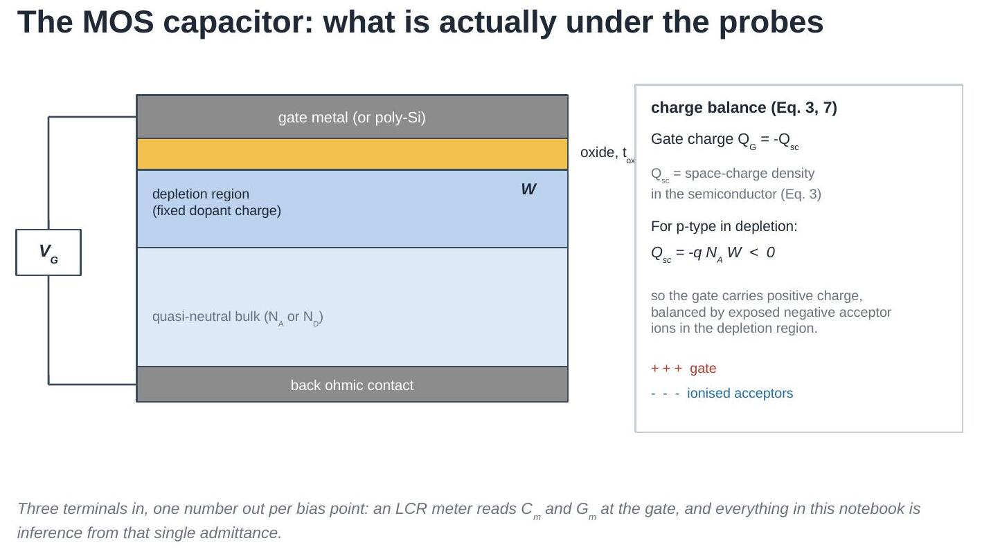
A MOS capacitor is a metal gate, a thin oxide, and a doped silicon substrate, with an ohmic contact on the back. The gate and the substrate are the two plates; the oxide is the dielectric between them - except that one of the two plates is a semiconductor, and a semiconductor's surface charge moves in response to the field the way a metal's never does.
The oxide capacitance is fixed by geometry alone:
This never changes with bias. Every feature in a C-V curve comes from the other plate: the semiconductor's depletion layer growing and shrinking underneath the gate, which changes the effective thickness of the dielectric between the gate and the bulk silicon. The two capacitances - fixed oxide, bias-dependent semiconductor - sit in series, and Eq. (1) is the one number on the whole curve you can check by inspection: it should match the flattest part of the plot in strong accumulation (Sec. 6).
tox_nm = 10.0        # oxide thickness
area_cm2 = 1e-4       # 100 um x 100 um gate pad
Cox_pa = cgv.oxide_capacitance_per_area(tox_nm)
Cox = cgv.oxide_capacitance(area_cm2, tox_nm)
print(f"C_ox (per area) = {Cox_pa*1e6:.2f} uF/cm^2")
print(f"C_ox (this device, A={area_cm2*1e8:.0f} um^2) = {Cox*1e12:.2f} pF")
C_ox (per area) = 0.35 uF/cm^2
C_ox (this device, A=10000 um^2) = 34.53 pF
3. What happens at the semiconductor surface as the gate bias changes?
Define the surface potential \(\phi_s\): the band bending at the
semiconductor-oxide interface, relative to the neutral bulk, with
\(\phi_s=0\) at flat band. This notebook works a p-type substrate as its
running example (n-type is a mirror image, and every function below takes
a dopant_type argument).
Sign convention - declared once, used everywhere below. For a p-type substrate:
- \(\phi_s < 0\) is accumulation: majority holes pulled to the surface.
- \(\phi_s > 0\) is depletion: holes pushed away, exposing ionised acceptors.
- \(\phi_s > 2\phi_F\) is (strong) inversion: enough band bending that the surface behaves as if it were n-type, where the bulk Fermi potential is
positive for p-type. Increasing the gate bias moves a p-type surface from accumulation toward inversion; for n-type it is the reverse, and \(\phi_F\) itself is negative.
This is the same band-bending picture the Kelvin probe / surface photovoltage notebook uses - there, \(\phi_s\) is inferred from a null voltage or from illumination; here, it is driven directly by an applied gate bias. The electrostatics underneath is identical.
4. Why is the semiconductor's share of the capacitance itself bias-dependent?
Solving Poisson's equation with Boltzmann statistics gives the exact semiconductor surface field, valid all the way from accumulation through depletion into inversion (not just the depletion approximation) [5]:
and, from Gauss's law, the space-charge density per unit area:
\(Q_{sc}\) is a decreasing function of \(\phi_s\): more band bending always drives the semiconductor's own charge more negative (positive in accumulation, negative in depletion, for p-type). The capacitance that matters is the gate's response, \(-Q_{sc}\), so
a differential quantity - the slope of Eq. (3), not the charge divided by the potential. Two useful checks: at flat band, \(C_s\) reduces to \(\varepsilon_s/L_D\), with the Debye length
and, well inside depletion (small \(\phi_s\), far from inversion), \(Q_{sc}\) matches the familiar depletion-approximation width
to a few percent. Both checks are in cgv_helper_checks.py.
Na = 1e16   # p-type substrate, cm^-3
phi_s = np.linspace(-0.4, 1.0, 400)
Qsc = cgv.space_charge_density(phi_s, Na, 'p')
Cs = cgv.semiconductor_capacitance(phi_s, Na, 'p')
phiF = cgv.fermi_potential(Na, 'p')

fig, (ax1, ax2) = plt.subplots(1, 2, figsize=(11, 4))
ax1.plot(phi_s, Qsc*1e6)
ax1.axvline(0, color='gray', lw=0.8)
ax1.axvline(2*phiF, color='gray', ls='--', lw=0.8)
ax1.set_xlabel(r'surface potential $\phi_s$ (V)')
ax1.set_ylabel(r'$Q_{sc}$ ($\mu$C/cm$^2$)')
ax1.set_title('space charge (Eq. 3)')

ax2.semilogy(phi_s, Cs*1e6)
ax2.axvline(0, color='gray', lw=0.8, label='flat band')
ax2.axvline(2*phiF, color='gray', ls='--', lw=0.8, label=r'$2\phi_F$ (inversion onset)')
ax2.set_xlabel(r'surface potential $\phi_s$ (V)')
ax2.set_ylabel(r'$C_s$ ($\mu$F/cm$^2$)')
ax2.set_title('semiconductor capacitance (Eq. 4)')
ax2.legend(fontsize=9)
plt.tight_layout()
plt.show()
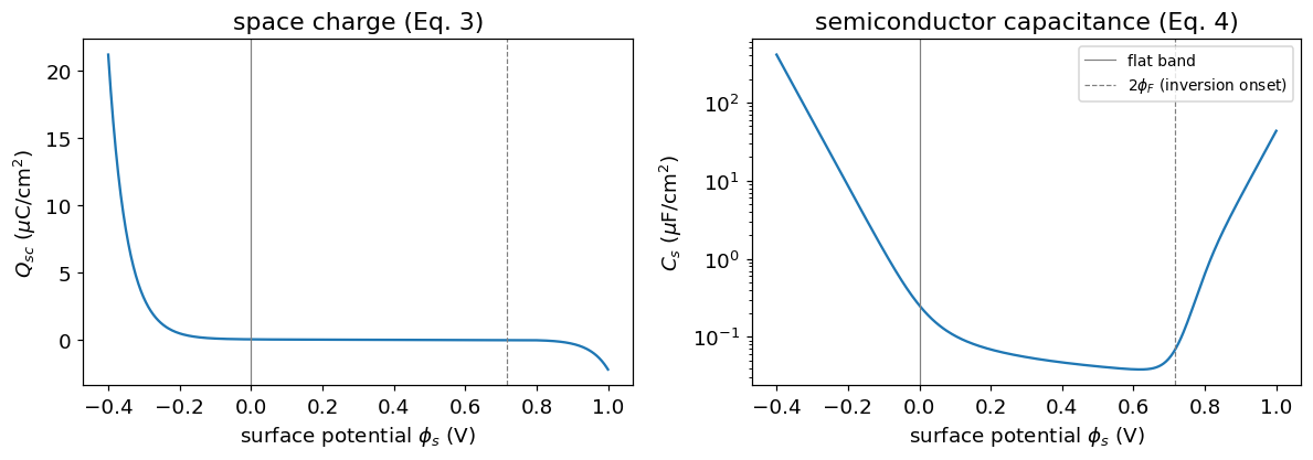
\(C_s\) spans nearly five decades between accumulation and depletion. Accumulation piles up majority carriers right at the interface, so a tiny change in \(\phi_s\) moves a lot of charge - \(C_s\) is huge, and the series combination in Sec. 6 will be dominated by \(C_{\text{ox}}\) alone. In depletion, \(C_s\) falls to the value set by the depletion width, which is why the total capacitance drops as the gate is biased away from accumulation. Past \(2\phi_F\), \(C_s\) turns back up as the exponentially growing minority-carrier (inversion) charge takes over from the slowly saturating depletion charge - and whether that turn-up shows up in a real measurement is entirely a question of frequency, which is Sec. 5.
5. Why does measurement frequency change the shape of the curve?
Majority carriers respond to the AC signal in about a dielectric relaxation time - picoseconds, effectively instantaneous. Minority carriers in the depletion region do not exist in equilibrium; they have to be generated, thermally, one electron-hole pair at a time, and that takes a generation lifetime - microseconds to milliseconds in a teaching-grade device. That mismatch is the whole reason C-V curves are measured at more than one frequency:
- High frequency (HF). The AC signal is far too fast for minority carriers to generate in step with it. Past the onset of inversion, the inversion charge is frozen at whatever the DC bias has managed to accumulate over the whole sweep, and \(C_s\) is clamped at its depletion-limited value.
- Low frequency / quasi-static (LF). The AC signal (or the DC ramp rate, if a true DC method is used instead) is slow enough that minority carriers keep up. The equilibrium \(C_s(\phi_s)\) of Eq. (4) - inversion turn-up included - is measured directly.
- Deep depletion. The bias sweep itself is faster than the generation lifetime, so the surface never reaches equilibrium at all: depletion keeps growing past where it would have stopped, and \(C\) falls below even the HF minimum.
Section 6 builds all three from the same underlying physics, differing only in what is allowed to happen to the minority-carrier charge.
6. What does the ideal C-V curve look like, feature by feature?
The oxide and the semiconductor combine in series:
with \(\phi_s(V)\) found from charge balance across the structure - the gate voltage splits between band bending and the voltage dropped across the oxide:
solved numerically for \(\phi_s\) at each \(V_G\) (surface_potential_from_bias).
\(V_{FB}\), the flat-band voltage, is the subject of Sec. 7; take it as a
given offset for now.
VFB = -0.9   # flat-band voltage, worked example
Vg = np.linspace(VFB - 3.0, VFB + 3.0, 400)

C_hf = cgv.hf_cv_curve(Vg, area_cm2, tox_nm, Na, 'p', VFB)
C_lf = cgv.lf_cv_curve(Vg, area_cm2, tox_nm, Na, 'p', VFB)
C_dd = cgv.deep_depletion_cv(Vg, area_cm2, tox_nm, Na, 'p', VFB)
VT = cgv.threshold_voltage(Cox_pa, Na, 'p', VFB)

fig, ax = plt.subplots(figsize=(7.6, 5))
ax.plot(Vg, C_lf*1e12, lw=2, color='C2', label='low frequency / quasi-static')
ax.plot(Vg, C_hf*1e12, lw=2, color='C0', label='high frequency (1 MHz)')
ax.plot(Vg, C_dd*1e12, lw=2, ls='--', color='C3',
        label='deep depletion (swept too fast)')
ax.axhline(Cox*1e12, color='gray', lw=0.8, ls='-')
ax.text(Vg[5], Cox*1e12*1.01, r'$C_{ox}$', fontsize=10, color='gray')
for x, name in ((VFB, r'$V_{FB}$'), (VT, r'$V_T$')):
    ax.axvline(x, color='gray', ls=':', lw=0.9)
    ax.annotate(name, (x, Cox*1e12*0.55), xytext=(4, 0),
                textcoords='offset points', fontsize=10, color='gray')
for x, name in ((VFB - 1.9, 'accumulation'), ((VFB + VT)/2, 'depletion'),
                (VT + 1.1, 'inversion')):
    ax.annotate(name, (x, Cox*1e12*0.13), ha='center', fontsize=10,
                color='0.35')
ax.set_ylim(0, Cox*1e12*1.12)
ax.set_xlabel(r'gate voltage $V_G$ (V)')
ax.set_ylabel('capacitance (pF)')
ax.set_title(r'Eqs. (7)-(8): p-type MOS, $N_A=10^{16}$ cm$^{-3}$, 10 nm oxide')
ax.legend(fontsize=9, loc='center left')
plt.tight_layout()
plt.show()

print(f"C_ox            = {Cox*1e12:7.2f} pF")
print(f"C_min (HF)      = {C_hf.min()*1e12:7.2f} pF   ratio C_min/C_ox = {C_hf.min()/Cox:.3f}")
print(f"C at V_FB       = {np.interp(VFB, Vg, C_hf)*1e12:7.2f} pF")
print(f"V_FB = {VFB:+.2f} V,  V_T = {VT:+.2f} V")
C_ox            =   34.53 pF
C_min (HF)      =    3.44 pF   ratio C_min/C_ox = 0.100
C at V_FB       =   14.62 pF
V_FB = -0.90 V,  V_T = -0.04 V
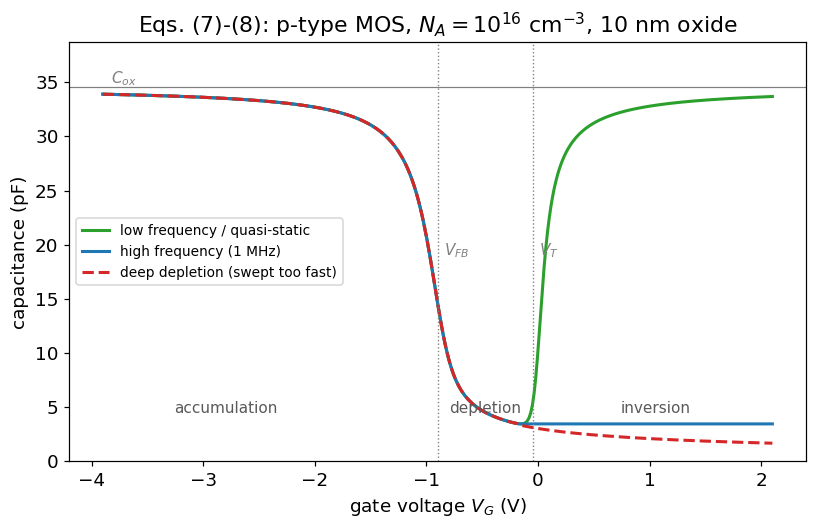
Three plateaus and a knee, read left to right. In strong accumulation, all three curves sit at \(C_{\text{ox}}\) (slightly below it, because a 10 nm oxide is thin enough that accumulation does not fully saturate - a real, literature-documented effect, not noise). Through depletion, all three fall together, because the physics is identical until minority carriers matter. Past the knee, they separate: HF freezes at a minimum set by the maximum depletion width; LF rises back toward \(C_{\text{ox}}\) as the inversion layer forms in step with the sweep; and deep depletion overshoots past the HF minimum because the surface never gets the chance to invert at all - it is not swept too fast in time, it is swept too fast relative to how slowly minority carriers generate. Comparing the HF and LF curves at fixed bias is itself a diagnostic: any difference beyond depletion is minority-carrier response, and its size is a rough clock on the generation lifetime.
7. Where does the voltage axis sit - flat-band voltage and oxide charge?
the metal-semiconductor work function difference \(\phi_{ms}\), minus the effective oxide charge divided by the oxide capacitance [2]. If the oxide carried no charge at all, \(V_{FB}\) would just be \(\phi_{ms}\); any additional shift is oxide charge, and Eq. (9) rearranges to read that charge back off a measured curve:
This is the section's own measured-vs-inferred moment: \(V_{FB}\) is read directly off a curve, \(Q_{\text{eff}}\) is inferred from how far that curve has moved relative to the charge-free ideal.
To find \(V_{FB}\) on a measured curve, compute the ideal flat-band capacitance from the Debye length at \(\phi_s=0\) - \(C_s(0)=\varepsilon_s/L_D\) combined in series with \(C_{\text{ox}}\) - and read off the bias where the measured HF curve crosses it.
Cfb_pa = cgv.flatband_capacitance_per_area(Cox_pa, Na)
Cfb = Cfb_pa * area_cm2
i_cross = np.argmin(np.abs(C_hf - Cfb))
VFB_read = Vg[i_cross]
print(f"C_FB = {Cfb*1e12:.3f} pF")
print(f"V_FB read off the curve = {VFB_read:.3f} V  (true value: {VFB:.3f} V)")

phi_ms = -0.85
Qeff = cgv.effective_oxide_charge(phi_ms, VFB_read, Cox_pa)
Neff = Qeff / cgv.Q
print(f"phi_ms (assumed) = {phi_ms:.3f} eV")
print(f"Q_eff = {Qeff*1e9:.3f} nC/cm^2  ->  N_eff = {Neff:.3e} cm^-2")
C_FB = 14.614 pF
V_FB read off the curve = -0.892 V  (true value: -0.900 V)
phi_ms (assumed) = -0.850 eV
Q_eff = 14.669 nC/cm^2  ->  N_eff = 9.156e+10 cm^-2
8. Where does inversion begin - threshold voltage?
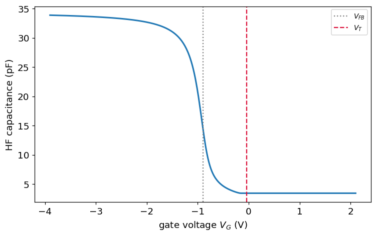
Threshold is defined as the bias at which \(\phi_s\) reaches \(2\phi_F\) - the conventional onset of strong inversion:
with \(s=+1\) for p-type (\(V_T>V_{FB}\), more depletion needed to invert) and \(s=-1\) for n-type (\(V_T<V_{FB}\)) [6]. On the HF curve, \(V_T\) sits close to (though not exactly at) the capacitance minimum - the true minimum is set by where the exact \(C_s(\phi_s)\) of Eq. (4) actually turns over, which is what Sec. 4's checks locate numerically rather than assume analytically.
VT = cgv.threshold_voltage(Cox_pa, Na, 'p', VFB)
print(f"V_T = {VT:.3f} V   (V_FB = {VFB:.3f} V)")

fig, ax = plt.subplots(figsize=(7, 4.5))
ax.plot(Vg, C_hf*1e12, lw=2)
ax.axvline(VFB, color='gray', ls=':', label=r'$V_{FB}$')
ax.axvline(VT, color='crimson', ls='--', label=r'$V_T$')
ax.set_xlabel(r'gate voltage $V_G$ (V)')
ax.set_ylabel('HF capacitance (pF)')
ax.legend(fontsize=9)
plt.tight_layout()
plt.show()
V_T = -0.043 V (V_FB = -0.900 V)
9. How do we turn C(V) into a doping profile?
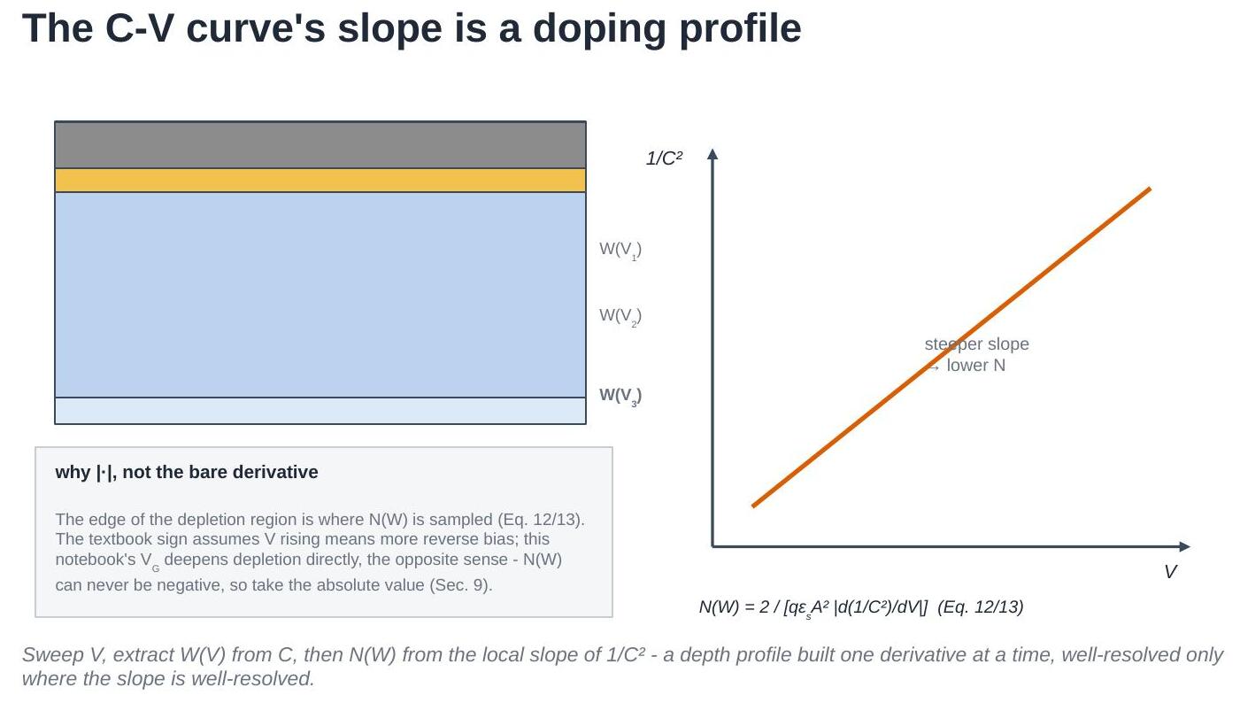
Differentiate the series combination and the algebra collapses to a single working formula [1]:
with a depth scale that comes straight from the measured capacitance alone:
The absolute value in Eq. (12) is deliberate, and worth dwelling on: the textbook form of this formula is usually written for a bias convention where increasing voltage means increasing reverse bias, so \(1/C^2\) falls as \(V\) rises. The convention used throughout this notebook has increasing \(V_G\) deepen depletion directly (for p-type), the opposite sign - so \(1/C^2\) rises with \(V_G\) here. \(N(W)\) itself can never be negative, so working with \(|d(1/C^2)/dV|\) sidesteps having to track which convention is in play. Get this wrong and the formula still runs; it just hands back a negative doping density, which is a very easy mistake to miss if you are not looking for it.
This is the notebook's TLM-equivalent section: a slope carries the physics, extracted point by point from noisy data, and a naive finite difference is a lot noisier than the underlying curve suggests. Compare a raw finite difference against a smoothed one on the same data.
N_true_uniform = 3e16
VFB2 = -0.8
Vg2 = np.linspace(VFB2 + 0.1, VFB2 + 1.4, 120)
C2 = cgv.synthetic_hf_cv(Vg2, area_cm2, tox_nm, N_true_uniform, 'p', VFB2,
                         noise_frac=0.01, seed=1)

# cox_F tells the extraction to subtract the oxide from the series
# combination before turning capacitance into depth - see Eq. (13).
W_raw, N_raw = cgv.doping_profile_from_cv(Vg2, C2, area_cm2, cox_F=Cox,
                                          smooth=False, mask_invalid=False)
W_all, N_all = cgv.doping_profile_from_cv(Vg2, C2, area_cm2, cox_F=Cox,
                                          smooth=True, mask_invalid=False)
W_ok,  N_ok  = cgv.doping_profile_from_cv(Vg2, C2, area_cm2, cox_F=Cox,
                                          smooth=True)

fig, ax = plt.subplots(1, 2, figsize=(12, 4.6), sharey=True)
ax[0].semilogy(W_raw*1e7, N_raw, '.', ms=4, alpha=0.45, color='C0',
               label='raw finite difference')
ax[0].semilogy(W_all*1e7, N_all, lw=1.8, color='C1', label='smoothed')
ax[0].axhline(N_true_uniform, color='k', ls='--', lw=1, label='true doping')
ax[0].set_title('as measured - note the tail')
ax[1].semilogy(W_ok*1e7, N_ok, lw=2, color='C1', label='smoothed, masked')
ax[1].axhline(N_true_uniform, color='k', ls='--', lw=1, label='true doping')
ax[1].set_title('with the saturated points removed')
bad = ~np.isfinite(N_ok)
if bad.any():
    ax[1].axvspan(np.nanmin(W_all[bad])*1e7, np.nanmax(W_all[bad])*1e7,
                  color='C3', alpha=0.12)
    ax[1].text(np.nanmean(W_all[bad])*1e7, 4e17, 'inversion:\nno depth\ninformation',
               ha='center', fontsize=9, color='C3')
for a in ax:
    a.set_xlabel('depth W (nm)')
    a.legend(fontsize=9, loc='upper left')
    a.set_ylim(1e16, 1e19)
ax[0].set_ylabel(r'N (cm$^{-3}$)')
plt.tight_layout()
plt.show()

print(f"true doping                 : {N_true_uniform:.2e} cm^-3")
print(f"median of all points        : {np.nanmedian(N_all):.2e} cm^-3")
print(f"median of the valid points  : {np.nanmedian(N_ok):.2e} cm^-3")
print(f"largest value, unmasked     : {np.nanmax(N_all):.2e} cm^-3  <- artefact")
print(f"largest value, masked       : {np.nanmax(N_ok):.2e} cm^-3")
print(f"points discarded            : {bad.sum()} of {len(N_ok)}")
true doping                 : 3.00e+16 cm^-3
median of all points        : 3.82e+16 cm^-3
median of the valid points  : 3.38e+16 cm^-3
largest value, unmasked     : 1.65e+19 cm^-3  <- artefact
largest value, masked       : 1.78e+17 cm^-3
points discarded            : 27 of 120
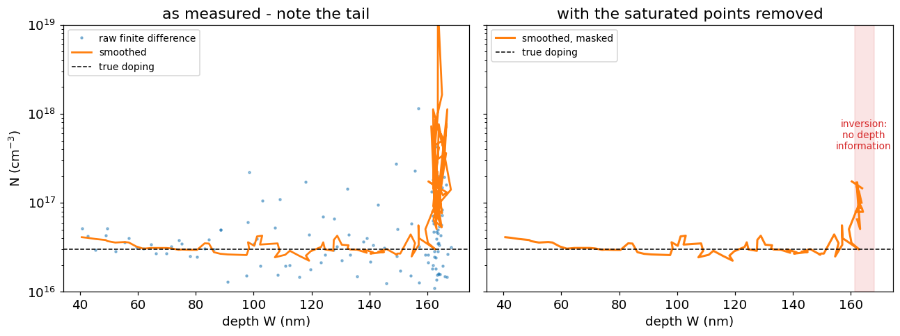
Uniform doping is the easy case: the answer is a horizontal line, and any wobble in it is noise. The technique earns its keep on a profile that is not uniform, because then \(N(W)\) is the measurement.
Building a believable test case takes more care than it looks. The depletion edge cannot be placed independently at each bias - it moves continuously, and the gate voltage has to account for the charge already uncovered. Integrating Poisson twice over an arbitrary \(N(x)\) gives both:
and then \(V_G = V_{FB} + \phi_s + Q_{dep}/C_{ox}\) as before. The second
integral is the depth-weighted first moment of the profile: charge
further from the surface costs more band bending, which is exactly why a
non-uniform profile is recoverable at all. cv_from_depth_profile does
this.
# a Gaussian implant sitting on a lightly doped substrate
depth = np.linspace(0, 6e-5, 8000)            # 0 - 600 nm, in cm
Rp, dRp = 6e-6, 2.2e-6                        # 60 nm projected range, 22 nm straggle
N_sub, N_peak = 2e16, 7e16
N_profile = N_sub + N_peak*np.exp(-0.5*((depth - Rp)/dRp)**2)

V_nu, C_nu = cgv.cv_from_depth_profile(depth, N_profile, area_cm2, tox_nm,
                                       'p', VFB2)

# sample it the way an instrument would, and add 0.5% noise
V_meas = np.linspace(V_nu.min() + 0.02, min(V_nu.max(), VFB2 + 4.0), 180)
C_meas = np.interp(V_meas, V_nu, C_nu)
C_meas = C_meas*(1 + np.random.default_rng(2).normal(0, 0.005, C_meas.shape))

W_ex, N_ex = cgv.doping_profile_from_cv(V_meas, C_meas, area_cm2,
                                        cox_F=Cox, smooth=True)

fig, ax = plt.subplots(1, 2, figsize=(12, 4.6))
ax[0].plot(V_meas, C_meas*1e12, '.', ms=4, color='C0')
ax[0].set_xlabel(r'$V_G$ (V)'); ax[0].set_ylabel('C (pF)')
ax[0].set_title('the C-V this profile produces')

ok = np.isfinite(N_ex) & np.isfinite(W_ex) & (W_ex > 1.5e-6)
ax[1].plot(depth*1e7, N_profile, 'k--', lw=1.5, label='true profile')
ax[1].plot(W_ex[ok]*1e7, N_ex[ok], lw=2, color='C1', label='recovered from C-V')
ax[1].set_xlim(0, 450); ax[1].set_ylim(0, 1.1e17)
ax[1].set_xlabel('depth W (nm)'); ax[1].set_ylabel(r'N (cm$^{-3}$)')
ax[1].set_title('implant over substrate, recovered')
ax[1].legend(fontsize=9)
plt.tight_layout()
plt.show()

pk = W_ex[ok][np.argmax(N_ex[ok])]
print(f"true peak     : {N_profile.max():.2e} cm^-3 at {Rp*1e7:.0f} nm")
print(f"recovered peak: {np.nanmax(N_ex[ok]):.2e} cm^-3 at {pk*1e7:.0f} nm")
print(f"true substrate: {N_sub:.2e} cm^-3")
print(f"recovered deep: {np.nanmedian(N_ex[ok][W_ex[ok] > 2.5e-5]):.2e} cm^-3")
true peak     : 9.00e+16 cm^-3 at 60 nm
recovered peak: 9.12e+16 cm^-3 at 64 nm
true substrate: 2.00e+16 cm^-3
recovered deep: 1.95e+16 cm^-3
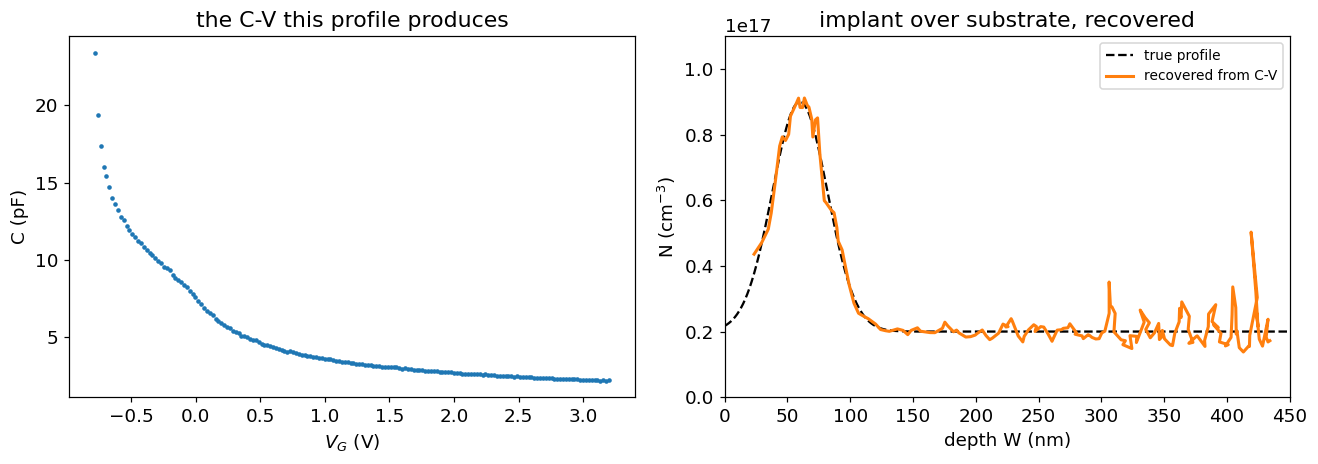
The peak comes back in the right place and close to the right height, and the substrate level is recovered beyond it. Two caveats worth carrying away.
The shallow end is missing. Nothing is recovered inside about 40 nm, because the depletion edge is never there: at flat band the surface is already depleted to a fraction of a Debye length, and the sweep can only push the edge outwards. C-V profiling cannot see the first few tens of nanometres, which is exactly where an implant peak often sits.
The recovered peak is lower and broader than the truth. Part of that is the smoothing filter, but the physical limit is the Debye length, about 40 nm at \(2\times10^{16}\) cm\(^{-3}\): majority carriers cannot follow a doping change faster than that, so the measured profile is the true one blurred over roughly \(3\lambda_D\). The depletion approximation used in Eq. (14) does not model that blurring, so the agreement here is slightly better than a real measurement would give. Eq. (5) is the relevant length.
10. What happens without an oxide? Schottky C-V and the Mott-Schottky line
Set \(C_{\text{ox}}\to\infty\) in Eqs. (7) and (12) - no series oxide element at all, a bare metal-semiconductor (Schottky) junction - and the general result collapses to the classic Mott-Schottky line:
linear in \(V\): the slope gives \(N\), the intercept on the voltage axis gives the built-in potential \(V_{bi}\) [1]. This is deliberately the same payoff KPSPV gives when SPV falls out of the CPD machinery as a special case - a general result specialising to a simpler, more famous one. It is also, structurally, the same fit TLM makes: a straight line whose slope is well-constrained by the data and whose intercept is a more fragile extrapolation.
The important check is that this is an algebraic identity, not a
numerical coincidence - the same helper code that builds the MOS curves
above, with Cox_pa set enormous, reproduces Eq. (15) exactly
(cgv_helper_checks.py, check 10).
N_schottky = 3e16
Vbi_true = 0.75
V_ms = np.linspace(-8, -0.2, 60)
C_ms = cgv.synthetic_mott_schottky(V_ms, N_schottky, Vbi_true, area_cm2, noise_frac=0.03, seed=3)

N_fit, N_fit_err, Vbi_fit, Vbi_fit_err = cgv.mott_schottky_fit(V_ms, C_ms, area_cm2)
print(f"N (true)   = {N_schottky:.3e} cm^-3")
print(f"N (fit)    = {N_fit:.3e} +/- {N_fit_err:.1e} cm^-3  ({100*N_fit_err/N_fit:.1f}%)")
print(f"Vbi (true) = {Vbi_true:.3f} V")
print(f"Vbi (fit)  = {Vbi_fit:.3f} +/- {Vbi_fit_err:.3f} V  ({100*Vbi_fit_err/Vbi_true:.1f}%)")

fig, ax = plt.subplots(figsize=(7, 5))
ax.plot(V_ms, 1/C_ms**2, 'o', ms=4, alpha=0.6, label='synthetic data (3% noise)')
fit_line = 2*(Vbi_fit - V_ms)/(cgv.Q*cgv.EPS_SI*area_cm2**2*N_fit)
ax.plot(V_ms, fit_line, lw=2, label='linear fit')
ax.set_xlabel('bias V (V)')
ax.set_ylabel(r'$1/C^2$ (F$^{-2}$)')
ax.set_title('Eq. (15): Mott-Schottky analysis')
ax.legend(fontsize=9)
plt.tight_layout()
plt.show()
N (true)   = 3.000e+16 cm^-3
N (fit)    = 3.013e+16 +/- 3.3e+14 cm^-3  (1.1%)
Vbi (true) = 0.750 V
Vbi (fit)  = 0.767 +/- 0.053 V  (7.1%)
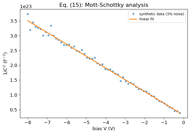
\(N\) comes back to within a percent or two of the noise level; \(V_{bi}\), extrapolated out to where the line crosses zero, carries a noticeably larger relative uncertainty for the same input noise - the slope is constrained by every point on the line, the intercept only by how far you have to extrapolate to reach it. Exactly the TLM lesson, in a different notebook.
11. What is the conductance method actually measuring?
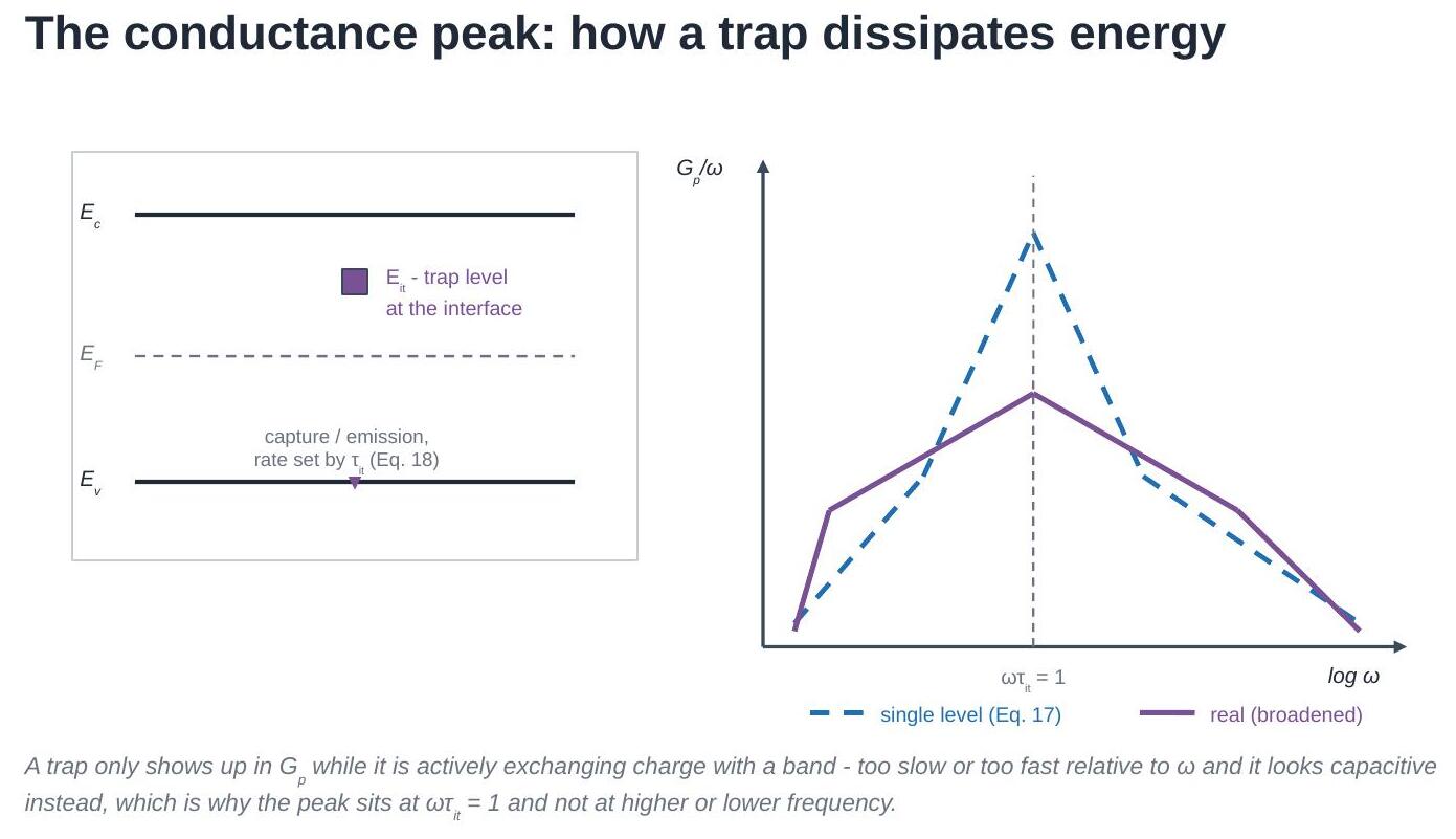
Interface states sit at energy levels inside the silicon band gap, right at the oxide interface. At a given bias, states near the Fermi level capture and emit carriers on some characteristic timescale \(\tau_{it}\). When the AC signal's angular frequency \(\omega\) is comparable to \(1/\tau_{it}\), the traps cannot quite keep up: their charging lags the signal, and that lag dissipates energy. A genuine loss mechanism - it shows up in \(G\), the out-of-phase component, not in \(C\).
The measured admittance at any one bias and frequency is
[3]. Sweep frequency at fixed bias, and the interface-trap signature is a peak in \(G_m/\omega\) - but only after removing the series oxide capacitance from the circuit, which is Sec. 12.
12. How do we get the semiconductor's true parallel conductance out of what the meter reports?
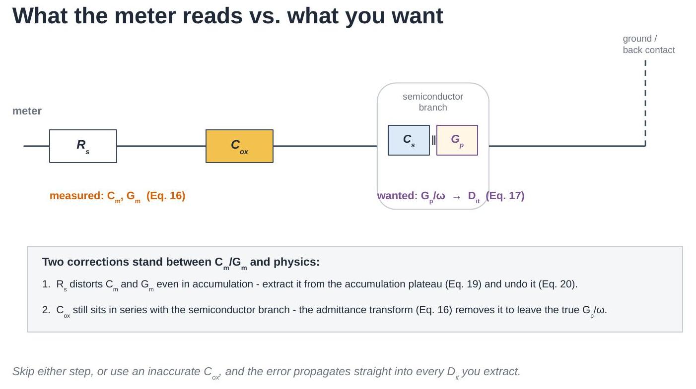
\(C_{\text{ox}}\) still sits in series with the semiconductor branch in the equivalent circuit, so the raw \(G_m/\omega\) is not yet the quantity that peaks cleanly with interface-trap physics. Converting the measured admittance through the known \(C_{\text{ox}}\) gives the semiconductor branch's true parallel conductance [3]:
Skipping this step, or using an inaccurate \(C_{\text{ox}}\), is the single biggest source of a wrong \(D_{it}\) - the error in \(C_{\text{ox}}\) propagates directly into Eq. (17) and from there directly into everything Sec. 13 extracts.
Dit_true = 5e11    # cm^-2 (areal density, single-level teaching model)
tau_it_true = 2e-5  # s
freqs = np.logspace(2, 6, 100)
Cm, Gm = cgv.synthetic_conductance_sweep(
    freqs, Dit_true, tau_it_true, area_cm2, tox_nm, noise_frac=0.02, seed=4)
omega = 2*np.pi*freqs
Gp_over_w = cgv.admittance_to_parallel(Cm, Gm, omega, Cox)

fig, ax = plt.subplots(figsize=(7, 5))
ax.semilogx(freqs, Gm/omega*1e12, 'o-', ms=3, alpha=0.5, label=r'raw $G_m/\omega$ (uncorrected)')
ax.semilogx(freqs, Gp_over_w*1e12, 'o-', ms=3, label=r'$G_p/\omega$ (Eq. 16, corrected)')
ax.set_xlabel('frequency (Hz)')
ax.set_ylabel(r'$G/\omega$ (pF)')
ax.legend(fontsize=9)
plt.tight_layout()
plt.show()
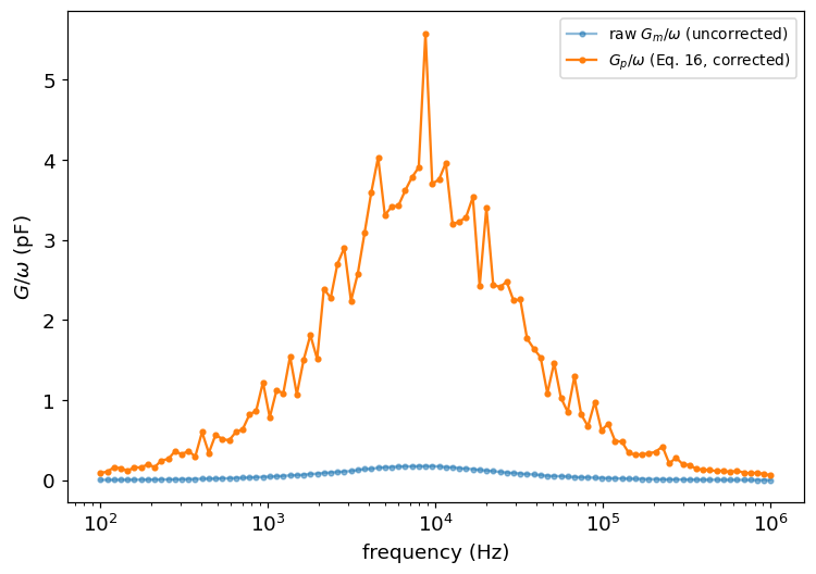
The corrected curve peaks at a lower frequency and a higher value than the raw one - the series \(C_{\text{ox}}\) shortens the semiconductor branch's effective time constant when left uncorrected, exactly as Sec. 12 warns. Only the corrected curve is the one Sec. 13 fits.
13. What does the conductance peak tell us about interface traps?
The simplest possible model - a single interface-trap energy level, no spread in time constant - gives a Lorentzian peak [3]:
peaking exactly at \(\omega\tau_{it}=1\) with height \(qD_{it}A/2\). The time constant itself is set by the capture rate:
with \(c_p=\sigma_pv_{th}\) the capture probability [3].
Eq. (18) is a teaching-grade starting point, not the full story. Real interface traps are spread over a continuum of energies, and real surfaces have patch-to-patch band-bending fluctuations - both broaden and lower the measured peak relative to what Eq. (18) predicts [3][2]. Nicollian and Brews give the full statistical treatment (a Gaussian average over band-bending fluctuations, their Eqs. 5.70-5.85); illustrating the effect without implementing that full double integral, superpose a spread of single-level peaks and watch the sum broaden and flatten relative to any one of them.
Dit_fit, tau_fit = cgv.fit_dit_from_peak(omega, Gp_over_w, area_cm2)
print(f"D_it (true) = {Dit_true:.3e} cm^-2")
print(f"D_it (fit)  = {Dit_fit:.3e} cm^-2  ({100*abs(Dit_fit-Dit_true)/Dit_true:.1f}% off)")
print(f"tau_it (true) = {tau_it_true:.2e} s")
print(f"tau_it (fit)  = {tau_fit:.2e} s")

# Illustrate broadening: superpose single-level peaks over a spread of tau
omega_grid = 2*np.pi*np.logspace(1, 8, 400)
taus = np.geomspace(tau_it_true/8, tau_it_true*8, 9)
single = cgv.conductance_lorentzian(omega_grid, Dit_true, tau_it_true, area_cm2)
broadened = np.mean(
    [cgv.conductance_lorentzian(omega_grid, Dit_true, t, area_cm2) for t in taus], axis=0)

fig, ax = plt.subplots(figsize=(7, 5))
ax.semilogx(omega_grid*tau_it_true, single*1e12, lw=2, label='single level (Eq. 17)')
ax.semilogx(omega_grid*tau_it_true, broadened*1e12, lw=2, ls='--',
            label='spread of time constants\n(illustrates the real, broader peak)')
ax.set_xlabel(r'$\omega\tau_{it}$')
ax.set_ylabel(r'$G_p/\omega$ (pF)')
ax.legend(fontsize=9)
plt.tight_layout()
plt.show()
D_it (true) = 5.000e+11 cm^-2
D_it (fit)  = 5.407e+11 cm^-2  (8.1% off)
tau_it (true) = 2.00e-05 s
tau_it (fit)  = 1.83e-05 s
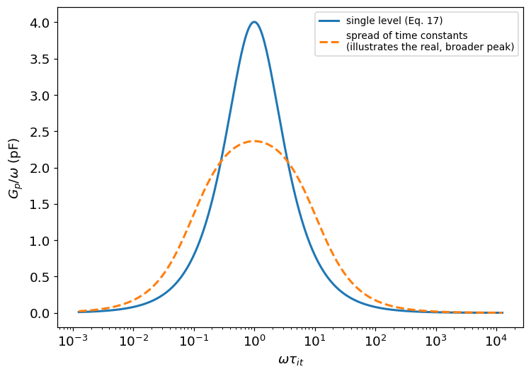
The broadened curve peaks lower and wider than the single-level model, for the same total trap density - reading \(D_{it}\) off Eq. (18)'s peak-height formula when the real peak is this broadened would underestimate \(D_{it}\). This is exactly the caution Nicollian and Brews give: the width of a measured \(G_p/\omega\) curve is itself information (about the spread of band-bending fluctuations across the surface, i.e. about surface uniformity), not just noise to average away.
14. How would you compute a C-V curve from scratch?
Everything so far has taken \(C_s(\phi_s)\) as given by Eq. (4), which was derived with Boltzmann statistics and fully ionised dopants. Both assumptions are good for moderately doped silicon at room temperature and both fail predictably: Boltzmann statistics overestimate the carrier density once the Fermi level approaches a band edge, and shallow dopants are not fully ionised at high concentration.
This section and the next three set the shortcuts aside and build the curve the way you would if you had to compute it properly. The chain is:
- solve bulk charge neutrality for \(E_F\),
- pick a surface potential \(\phi_s\) and get the carrier densities there,
- integrate Poisson once to get \(Q_s\),
- differentiate to get \(C_s\),
- balance the charge across the structure to get the \(V_G\) that produced that \(\phi_s\),
- sweep \(\phi_s\) and plot.
Note the direction. Sec. 6 solved Eq. (8) for \(\phi_s\) at each \(V_G\), which needs a root find at every point. Sweeping \(\phi_s\) instead makes every quantity an explicit function of it, and the curve comes out parametrically with no root finding at all.
Carrier densities. With Fermi-Dirac statistics the densities are Fermi integrals rather than exponentials:
normalised so that \(\mathcal{F}_j(\eta)\to e^{\eta}\) when \(\eta \ll 0\), which recovers Eq. (2)'s Boltzmann form exactly.
Ionisation. A dopant atom is only charged when its level is empty (donor) or full (acceptor), and that occupancy depends on where \(E_F\) sits relative to the level:
Neutrality. The bulk must be neutral, which fixes \(E_F\):
NA_demo = 1e16

Ef = cgv.bulk_fermi_level(NA_demo, 0.0)          # Eq. (23)
n_b, p_b = cgv.carrier_densities_fd(Ef)          # Eq. (20)
NA_ion, _ = cgv.ionised_dopants(Ef, NA_demo, 0.0)  # Eq. (22)

print(f"N_A = {NA_demo:.1e} cm^-3")
print(f"  E_F - E_i        = {Ef:+.5f} eV   (Fermi-Dirac, Eq. 23)")
print(f"  -phi_F Boltzmann = {-cgv.fermi_potential(NA_demo,'p'):+.5f} eV   (Eq. 2)")
print(f"  difference       = {abs(Ef + cgv.fermi_potential(NA_demo,'p'))*1e3:.1f} meV")
print(f"  p = {p_b:.4e},  n = {n_b:.4e} cm^-3")
print(f"  ionised acceptors: {NA_ion/NA_demo*100:.2f} %")

eta = np.linspace(-12, 6, 200)
F_half = cgv.fermi_dirac_integral(0.5, eta)      # Eq. (21)

fig, ax = plt.subplots(1, 2, figsize=(12, 4.4))
ax[0].semilogy(eta, F_half, lw=2, label=r'$\mathcal{F}_{1/2}(\eta)$')
ax[0].semilogy(eta, np.exp(eta), '--', lw=1.5, label=r'$e^{\eta}$ (Boltzmann)')
ax[0].set_xlabel(r'$\eta = (E_F-E_c)/kT$'); ax[0].set_ylabel('normalised density')
ax[0].set_title('Eq. (21): the Fermi integral and its Boltzmann limit')
ax[0].legend(fontsize=9); ax[0].set_ylim(1e-6, 1e3)

Nd = np.logspace(14, 20, 40)
frac = [cgv.ionised_dopants(cgv.bulk_fermi_level(N, 0.0), N, 0.0)[0]/N for N in Nd]
ax[1].semilogx(Nd, np.array(frac)*100, lw=2, color='C1')
ax[1].axhline(100, color='gray', ls='--', lw=0.8)
ax[1].set_xlabel(r'$N_A$ (cm$^{-3}$)'); ax[1].set_ylabel('ionised acceptors (%)')
ax[1].set_title('Eq. (22): full ionisation is an approximation')
ax[1].set_ylim(0, 105)
plt.tight_layout(); plt.show()
N_A = 1.0e+16 cm^-3
  E_F - E_i        = -0.35212 eV   (Fermi-Dirac, Eq. 23)
  -phi_F Boltzmann = -0.35808 eV   (Eq. 2)
  difference       = 6.0 meV
  p = 9.9634e+15,  n = 1.3574e+04 cm^-3
  ionised acceptors: 99.63 %
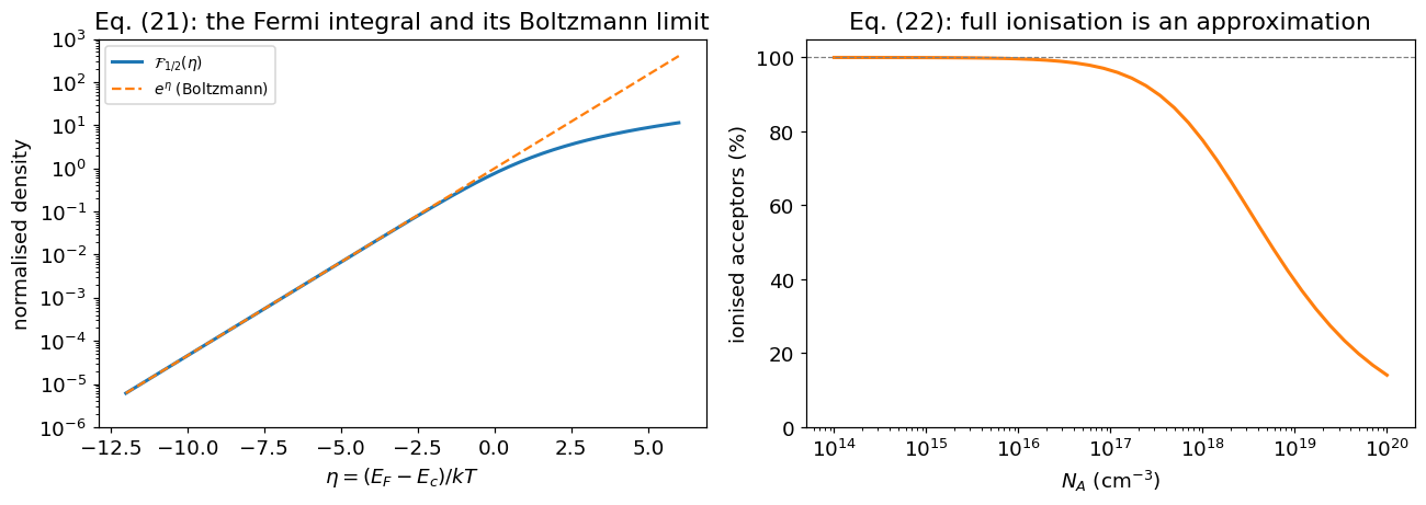
Two things to take from this.
The Boltzmann shortcut is good where we have been using it. At \(10^{16}\) cm\(^{-3}\) the Fermi level differs by about 6 meV from \(-\phi_F = -V_t\ln(N_A/n_i)\), and 99.6% of the acceptors are ionised. Nothing in Secs. 1-13 is materially wrong.
It stops being good exactly where devices get interesting. By \(10^{19}\) cm\(^{-3}\) only about 40% of the acceptors are ionised, and \(\mathcal{F}_{1/2}\) has fallen a factor of twenty below \(e^{\eta}\). A heavily doped substrate, a poly-Si gate, or the peak of an implant all sit in that regime, and a C-V analysis that assumes \(N = N_A\) there is reading the wrong number.
15. What does the space charge look like without the Boltzmann shortcut?
With the densities in hand, integrating Poisson's equation once from the neutral bulk to the surface gives the surface field, and Gauss's law turns that into the charge:
Every term inside the integral is a function of the local band bending \(\phi\), because bending the bands shifts each band edge and each dopant level relative to the fixed \(E_F\). Eq. (3) is what this collapses to when the two Fermi integrals become exponentials and the dopants are taken as fully ionised.
The capacitance is the derivative, with the same minus sign as Eq. (4):
and this is where the high-frequency distinction of Sec. 5 becomes a concrete instruction rather than a description: at high frequency the minority carriers are dropped from the derivative, because they cannot be generated fast enough to follow the AC signal. They are not dropped from \(Q_s\) itself, which is a DC quantity and sets the bias point. Freeze them in both places and the inversion branch comes out wrong.
phi_grid = np.linspace(-0.30, 0.95, 90)

Qs_fd = cgv.space_charge_density_fd(phi_grid, NA_demo, 0.0)        # Eq. (24)
Qs_bz = cgv.space_charge_density(phi_grid, NA_demo, 'p')           # Eq. (3)
Cs_lf = cgv.semiconductor_capacitance_fd(phi_grid, NA_demo, 0.0)   # Eq. (25)
Cs_hf = cgv.semiconductor_capacitance_fd(phi_grid, NA_demo, 0.0,
                                         minority_frozen=True)
Cs_bz = cgv.semiconductor_capacitance(phi_grid, NA_demo, 'p')      # Eq. (4)

fig, ax = plt.subplots(1, 2, figsize=(12, 4.6))
ax[0].semilogy(phi_grid, np.abs(Qs_fd)*1e6, lw=2, label='Fermi-Dirac, Eq. (24)')
ax[0].semilogy(phi_grid, np.abs(Qs_bz)*1e6, '--', lw=1.6,
               label='Boltzmann, Eq. (3)')
ax[0].axvline(0, color='gray', lw=0.8)
ax[0].set_xlabel(r'$\phi_s$ (V)'); ax[0].set_ylabel(r'$|Q_s|$ ($\mu$C/cm$^2$)')
ax[0].set_title('space charge'); ax[0].legend(fontsize=9)

ax[1].semilogy(phi_grid, Cs_lf*1e6, lw=2, label='FD, all carriers (LF)')
ax[1].semilogy(phi_grid, Cs_hf*1e6, lw=2, label='FD, minority frozen (HF)')
ax[1].semilogy(phi_grid, Cs_bz*1e6, '--', lw=1.4, color='k',
               label='Boltzmann, Eq. (4)')
ax[1].axvline(0, color='gray', lw=0.8)
ax[1].set_xlabel(r'$\phi_s$ (V)'); ax[1].set_ylabel(r'$C_s$ ($\mu$F/cm$^2$)')
ax[1].set_title('semiconductor capacitance'); ax[1].legend(fontsize=9)
plt.tight_layout(); plt.show()

for ps in (-0.20, 0.20, 0.60, 0.80):
    qf = float(cgv.space_charge_density_fd(ps, NA_demo, 0.0)[0])
    qb = float(np.atleast_1d(cgv.space_charge_density(ps, NA_demo, 'p'))[0])
    print(f"phi_s = {ps:+.2f} V:  Q_s(FD) = {qf:+.4e},  Q_s(Boltz) = {qb:+.4e}"
          f"   ({abs(qf/qb-1)*100:5.1f} % apart)")
phi_s = -0.20 V:  Q_s(FD) = +4.1813e-07,  Q_s(Boltz) = +4.4247e-07   (  5.5 % apart)
phi_s = +0.20 V:  Q_s(FD) = -2.4044e-08,  Q_s(Boltz) = -2.4044e-08   (  0.0 % apart)
phi_s = +0.60 V:  Q_s(FD) = -4.3673e-08,  Q_s(Boltz) = -4.3668e-08   (  0.0 % apart)
phi_s = +0.80 V:  Q_s(FD) = -7.5936e-08,  Q_s(Boltz) = -6.9049e-08   ( 10.0 % apart)
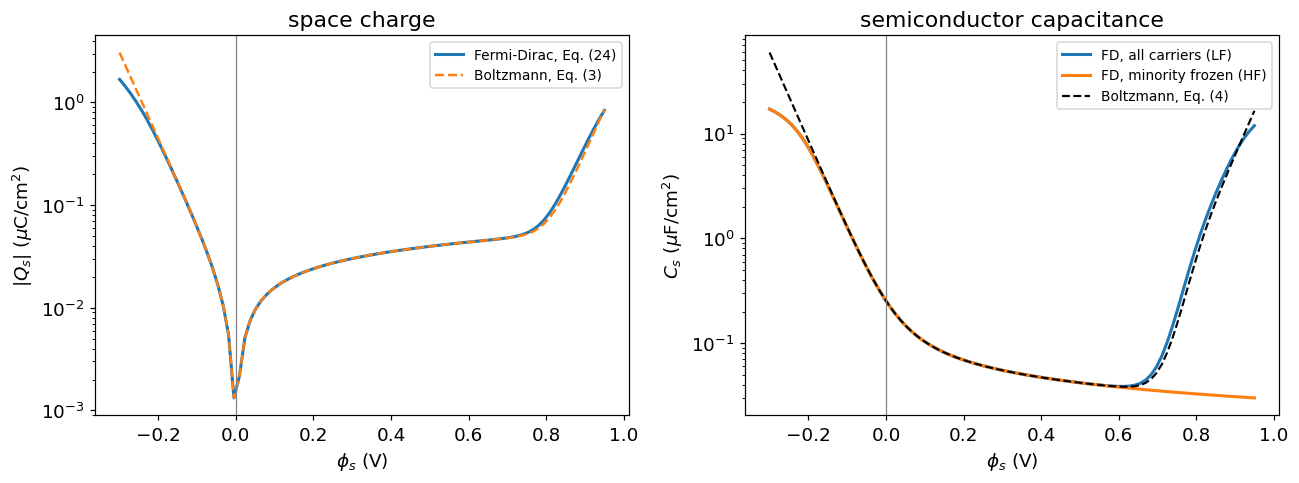
In depletion the two curves lie on top of each other - the charge there is ionised dopants, and the statistics of the free carriers barely matter. They separate at both ends, and for the same reason in each case: the surface has become degenerate, and the Boltzmann exponential overestimates how many carriers are really there. In accumulation at \(-0.2\) V the Boltzmann charge is about 6% too high; in strong inversion at \(+0.8\) V, about 10%.
The right-hand panel shows the high-frequency freeze doing its job. Below threshold the three curves agree. Past it the low-frequency curve turns sharply upward as the inversion layer forms, while the high-frequency curve stays flat - the same \(C_{min}\) plateau seen in every measured HF C-V curve, here produced by dropping one term from a derivative rather than by asserting it.
16. Putting it together: the full gate-voltage balance
Step 5 of the procedure is a charge balance across the whole structure. Everything the gate has to mirror - the semiconductor charge, the charge trapped at the interface, and the fixed charge inside the oxide - shows up as a shift of the voltage axis:
Eq. (9) is this equation with \(Q_{it}\) and \(Q_s\) folded into a single \(Q_{eff}\) and evaluated at flat band. Written out, two things it hides become visible.
The centroid factor. \(d\) is the position of the fixed charge measured from the oxide-semiconductor interface towards the gate, running from \(0\) to \(-t_i\). The weight \((1+d/t_i)\) is therefore 1 for charge sitting right at the semiconductor surface and 0 for charge at the gate. Fixed charge only shifts the curve to the extent that it is separated from the semiconductor. Charge at the interface still bends the bands, but it contributes nothing to \(V_G\); charge at the gate does nothing at all. This is the same centroid weighting that governs how much a given \(Q_f\) moves a Kelvin probe reading.
\(Q_{it}\) moves as the bands bend. Interface traps charge and discharge as \(E_F\) sweeps past them at the surface, so \(Q_{it}\) is a function of \(\phi_s\), not a constant. With donor-like states in the lower half of the gap and acceptor-like states in the upper half:
with the occupancy from Shockley-Read-Hall statistics evaluated with the surface densities:
That \(\phi_s\)-dependence is what stretches a measured C-V curve out along the voltage axis: charge going into traps has to be supplied by the gate too, so more voltage is needed for the same band bending.
phi_cv = np.linspace(-0.32, 0.95, 110)
phi_ms = -0.9

def half_c_voltage(V, C, C_half):
    """the gate voltage at which the curve crosses C_half - a robust,
    monotonic way to measure how far a curve has shifted."""
    o = np.argsort(C)
    return np.interp(C_half, C[o], V[o])

Vg_id, C_id, _, _, _ = cgv.cv_curve_fd(phi_cv, area_cm2, tox_nm, NA_demo, 0.0,
                                       phi_ms_eV=phi_ms, high_frequency=True)

# 1e12 cm^-2 of positive fixed charge - a poor oxide, not a clean one
Qf = 1e12*cgv.Q
Vg_s, C_s, _, _, _ = cgv.cv_curve_fd(phi_cv, area_cm2, tox_nm, NA_demo, 0.0,
                                     phi_ms_eV=phi_ms, Qf_C_cm2=Qf,
                                     centroid_cm=0.0, high_frequency=True)
Vg_g, C_g, _, _, _ = cgv.cv_curve_fd(phi_cv, area_cm2, tox_nm, NA_demo, 0.0,
                                     phi_ms_eV=phi_ms, Qf_C_cm2=Qf,
                                     centroid_cm=-0.9*tox_nm*1e-7,
                                     high_frequency=True)

# a bad interface: U-shaped D_it, donor-like below mid-gap, acceptor-like above
Eg = cgv.EG_SI_EV
def dit_shape(E, mid=1e12, edge=1e13, tail=0.15):
    E = np.asarray(E, float)
    return mid*(edge/mid)**np.exp(-np.minimum(E, Eg-E)/tail)
d_don = lambda E: np.where(np.asarray(E) < Eg/2, dit_shape(E), 0.0)
d_acc = lambda E: np.where(np.asarray(E) >= Eg/2, dit_shape(E), 0.0)
Vg_it, C_it_, _, _, Qit = cgv.cv_curve_fd(phi_cv, area_cm2, tox_nm, NA_demo,
                                          0.0, phi_ms_eV=phi_ms,
                                          Dit_donor=d_don, Dit_acceptor=d_acc,
                                          high_frequency=True)

C_half = 0.5*Cox
fig, ax = plt.subplots(1, 2, figsize=(12, 4.6))
ax[0].plot(Vg_id, C_id*1e12, lw=2, label='ideal')
ax[0].plot(Vg_s, C_s*1e12, lw=2, ls='--',
           label=r'$Q_f$ at the Si interface ($d=0$)')
ax[0].plot(Vg_g, C_g*1e12, lw=2, ls=':',
           label=r'same $Q_f$ near the gate ($d=-0.9\,t_i$)')
ax[0].set_title(r'Eq. (26): where $Q_f$ sits decides how much it shifts $V_G$')

ax[1].plot(Vg_id, C_id*1e12, lw=2, label=r'$D_{it}=0$')
ax[1].plot(Vg_it, C_it_*1e12, lw=2, ls='--',
           label=r'U-shaped $D_{it}$, $10^{12}$ cm$^{-2}$eV$^{-1}$ mid-gap')
ax[1].set_title('Eqs. (27)-(28): interface traps stretch the curve')
for a in ax:
    a.set_xlim(-2.6, 0.8); a.set_xlabel(r'$V_G$ (V)'); a.set_ylabel('C (pF)')
    a.axhline(C_half*1e12, color='gray', lw=0.7, ls='-.')
    a.legend(fontsize=8.5, loc='lower left')
plt.tight_layout(); plt.show()

v0 = half_c_voltage(Vg_id, C_id, C_half)
print(f"Q_f = 1e12 cm^-2 on C_ox = {Cox_pa*1e6:.3f} uF/cm^2")
print(f"  ideal curve crosses C_ox/2 at            {v0:+.3f} V")
print(f"  charge at the Si interface (d=0)         {half_c_voltage(Vg_s,C_s,C_half)-v0:+.3f} V shift")
print(f"  same charge at 0.9 t_i from the interface{half_c_voltage(Vg_g,C_g,C_half)-v0:+.3f} V shift")
print(f"  textbook Q_f/C_ox                        {-Qf/Cox_pa:+.3f} V")
print(f"\n  D_it stretch: 90%-to-10% of C_ox takes "
      f"{abs(half_c_voltage(Vg_id,C_id,0.9*Cox)-half_c_voltage(Vg_id,C_id,0.1*Cox)):.3f} V ideal, "
      f"{abs(half_c_voltage(Vg_it,C_it_,0.9*Cox)-half_c_voltage(Vg_it,C_it_,0.1*Cox)):.3f} V with traps")
print(f"  Q_it swings {Qit.min()/cgv.Q:.2e} .. {Qit.max()/cgv.Q:.2e} q/cm^2 across the sweep")
Q_f = 1e12 cm^-2 on C_ox = 0.345 uF/cm^2
  ideal curve crosses C_ox/2 at            -0.942 V
  charge at the Si interface (d=0)         -0.464 V shift
  same charge at 0.9 t_i from the interface-0.046 V shift
  textbook Q_f/C_ox                        -0.464 V

  D_it stretch: 90%-to-10% of C_ox takes 1.333 V ideal, 1.872 V with traps
  Q_it swings -1.19e+12 .. 1.24e+12 q/cm^2 across the sweep
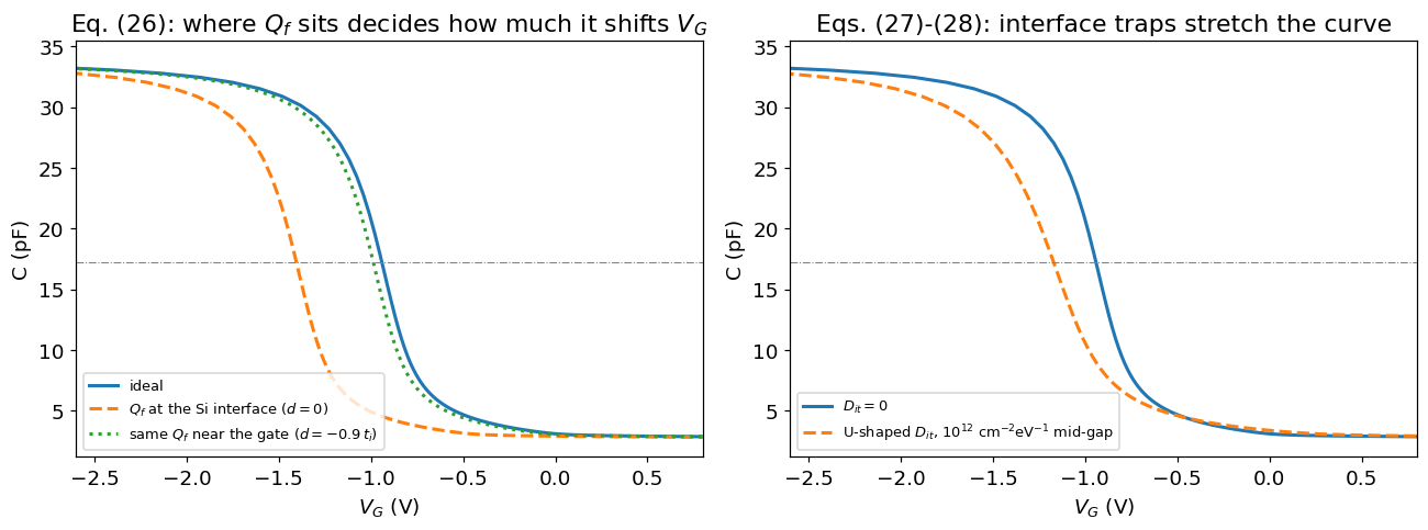
The left panel makes the centroid concrete. The same \(10^{12}\) cm\(^{-2}\) of positive charge shifts the curve by about half a volt when it sits against the silicon, and by a tenth of that when it sits against the gate. The full shift matches the textbook \(Q_f/C_{ox}\) only in the first case, which is the case that expression silently assumes. An extracted \(Q_{\text{eff}}\) from Eq. (10) is really the product \(Q_f(1+d/t_i)\), and a C-V measurement on its own cannot separate the two - the same ambiguity a Kelvin probe has.
The right panel shows the trap stretch. The curve is not shifted so much as sheared: in depletion, where \(E_F\) is sweeping through the middle of the gap, the traps charge and discharge and absorb gate charge, so more volts are needed per volt of band bending. The accumulation-to-inversion transition is drawn out measurably. That stretch is the C-V signature of a bad interface, and quantifying it is what the Terman method does - though the conductance method of Secs. 11-13 is more sensitive, because it measures the loss rather than a distortion of the shape.
17. What if the charge is not uniform, and what the full trap admittance looks like
Two loose ends from the model above, both of which matter on real films.
Fixed charge is not uniform across the gate. A dielectric deposited over a wafer has a distribution of \(Q_f\), not a single value, and a large-area gate averages over it. Sampling \(Q_f' = Q_f + \Delta q\) from a Gaussian and re-solving Eq. (26) for each sample gives a distribution \(P(\phi_s)\) at every bias, and the measured curve is the average over it. The visible effect is a smearing of every feature - and, importantly, it looks exactly like a higher \(D_{it}\), which is the trap.
The interface-state admittance has more branches than Eq. (18). A trap can exchange carriers with either band, so the equivalent circuit has a capture resistance to each:
together with the trap's own capacitance
Integrating each branch over the gap gives six frequency-dependent quantities - \(C_{dp}, C_{dn}, C_{pn}\) and \(G_{dp}, G_{dn}, G_{pn}\) - of the form
and the measurable trap-response conductance is \(G_p = G_{dp} + G_{dn}\). Eq. (18)'s single-level Lorentzian is this with \(D_{it}\) a delta function and one capture path dominating.
# --- the conductance peak, computed from the full branch model ---
Dit_flat = lambda E: np.full_like(np.asarray(E, float), 1e11)
freq = np.logspace(0, 7, 220)
omega_f = 2*np.pi*freq

fig, ax = plt.subplots(1, 2, figsize=(12, 4.6))
for ps, c in zip((0.10, 0.15, 0.20, 0.25, 0.30), ['C0','C1','C2','C3','C4']):
    br = cgv.interface_branch_admittance(omega_f, ps, Dit_flat, NA_demo, 0.0)
    Gp = cgv.interface_conductance_parallel(br)          # Eqs. (29)-(31)
    ax[0].semilogx(freq, Gp/omega_f*1e9, lw=1.8, color=c,
                   label=rf'$\phi_s$ = {ps:.2f} V')
ax[0].set_xlabel('frequency (Hz)')
ax[0].set_ylabel(r'$G_p/\omega$ (nF/cm$^2$)')
ax[0].set_title('Eq. (31): the peak scans with bias')
ax[0].legend(fontsize=8.5)

# --- what a fluctuating Q_f does to the curve ---
sig_q = 4e11*cgv.Q
Vg_sm = np.linspace(-2.6, 0.6, 60)
C_sharp = np.interp(Vg_sm, Vg_id, C_id)
C_smear = np.empty_like(Vg_sm)
for i, v in enumerate(Vg_sm):
    ps_samp, wts = cgv.phi_s_distribution(v, Cox_pa, phi_ms, 0.0, sig_q,
                                          NA_demo, 0.0, n_points=15)
    Cs_samp = cgv.semiconductor_capacitance_fd(ps_samp, NA_demo, 0.0,
                                               minority_frozen=True)
    C_smear[i] = np.sum(wts*cgv.total_capacitance_series_per_area(Cox_pa, Cs_samp))*area_cm2
ax[1].plot(Vg_sm, C_sharp*1e12, lw=2, label='uniform $Q_f$')
ax[1].plot(Vg_sm, C_smear*1e12, lw=2, ls='--',
           label=r'$\sigma_q = 4\times10^{11}$ q/cm$^2$')
ax[1].set_xlabel(r'$V_G$ (V)'); ax[1].set_ylabel('C (pF)')
ax[1].set_title('charge non-uniformity smears the curve')
ax[1].legend(fontsize=9)
plt.tight_layout(); plt.show()

for ps in (0.10, 0.20, 0.30):
    br = cgv.interface_branch_admittance(omega_f, ps, Dit_flat, NA_demo, 0.0)
    Gw = cgv.interface_conductance_parallel(br)/omega_f
    print(f"phi_s = {ps:.2f} V -> G_p/omega peaks at {freq[np.argmax(Gw)]:.2e} Hz")
phi_s = 0.10 V -> G_p/omega peaks at 7.22e+04 Hz
phi_s = 0.20 V -> G_p/omega peaks at 1.46e+03 Hz
phi_s = 0.30 V -> G_p/omega peaks at 3.42e+01 Hz
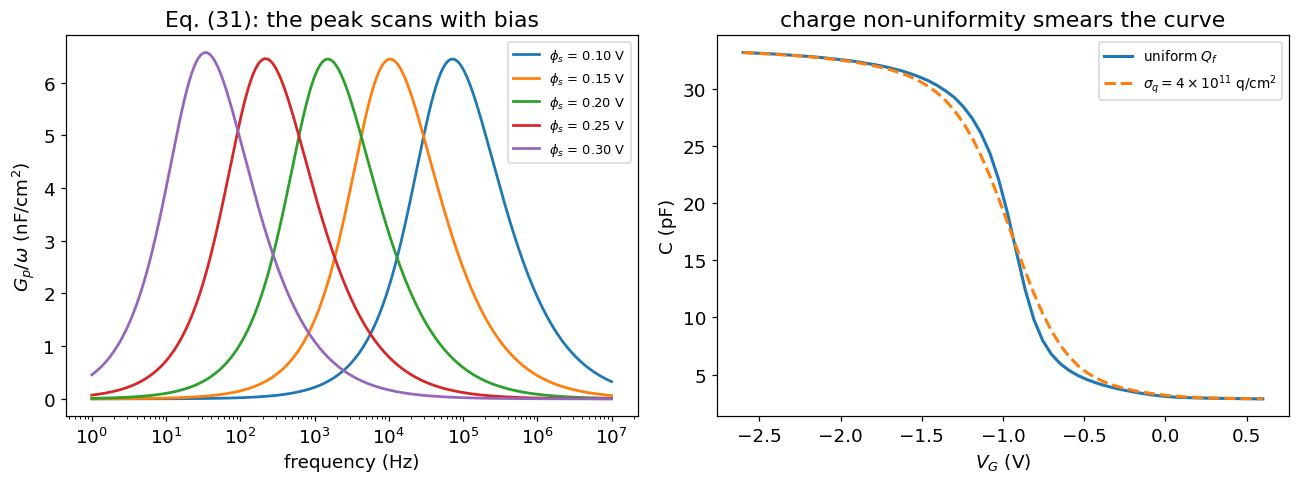
The left panel is the conductance method in one picture. Each curve is the same interface, the same \(D_{it}\), measured at a different bias. The peak moves through four decades of frequency as the surface potential changes by 0.2 V, because the time constant \(\tau_p = 1/(\sigma_p v_{th} p_s)\) follows the surface hole density, and that is exponential in \(\phi_s\). Reading the peak frequency at each bias maps the trap time constant through the gap; reading the peak height gives \(D_{it}\) there.
The right panel is the warning that goes with it. A film whose fixed charge varies by \(4\times10^{11}\) q/cm\(^{-2}\) across the gate produces a visibly gentler transition, and nothing about the shape says the cause was non-uniformity rather than interface traps. Two independent measurements - or a smaller gate - are the only way to tell them apart.
18. What ruins a real measurement, and how do you know?
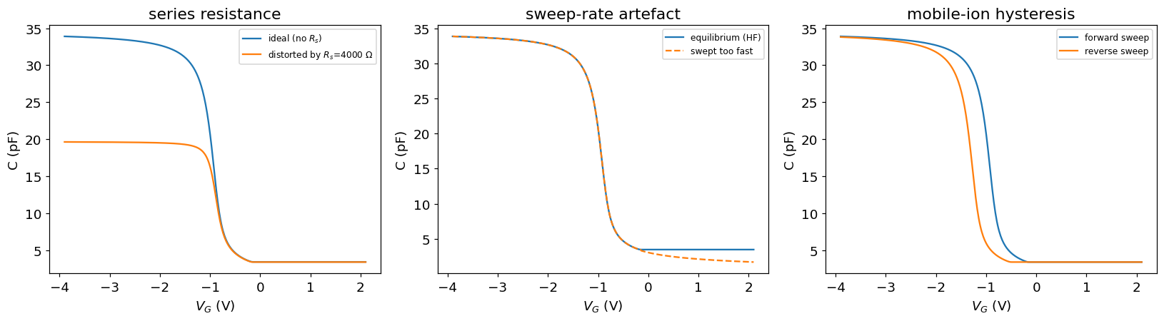
Three distinct non-idealities. They are commonly confused with each other, and telling them apart is the actual skill this section teaches.
Series resistance. Contact and substrate spreading resistance distort both \(C_m\) and \(G_m\), worst in strong accumulation at high frequency, where the device looks almost purely resistive. Extract it there [4]:
then correct the rest of the sweep:
Left uncorrected, \(R_s\) can make even \(C_{\text{ox}}\) itself read low.
Sweep-rate artefacts. Already met in Sec. 6 as deep depletion: a bias swept faster than the minority-carrier generation lifetime never reaches the equilibrium LF curve.
Mobile ionic charge. Sodium or potassium ions drifting under bias (or worse, under bias-temperature stress) shift \(V_{FB}\) between a forward and a reverse sweep - hysteresis. The shift gives the mobile sheet density directly:
The minus sign matters: positive mobile ions (Na\(^+\), K\(^+\)) that drift to the oxide-semiconductor interface between the forward and reverse sweep make \(V_{FB}\) more negative on the reverse sweep - the same relationship as Eq. (9), where a more positive \(Q_{\text{eff}}\) pulls \(V_{FB}\) down. Dropping the sign would report a negative ion density for a real, physically positive contamination level.
These three do not look alike, and should not be confused. Series resistance distorts the curve's shape at a fixed bias history. A sweep-rate artefact changes the inversion plateau, not the depletion slope. Mobile-ion hysteresis shifts the whole curve sideways, by a different amount on the way up than on the way down, and is the only one of the three that depends on sweep direction at all.
fig, axes = plt.subplots(1, 3, figsize=(15, 4.3))

# --- series resistance ---
Rs_true = 4000.0   # a poorly contacted wafer; see the note below
f_test = 1e6
omega_t = 2*np.pi*f_test
Cm_ideal = C_hf  # reuse the Sec. 6 HF curve as the "ideal" device
Gm_ideal = np.full_like(Cm_ideal, 1e-9)
Zmeas = Rs_true + 1/(Gm_ideal + 1j*omega_t*Cm_ideal)
Ymeas = 1/Zmeas
Gm_meas, Cm_meas = Ymeas.real, Ymeas.imag/omega_t
axes[0].plot(Vg, Cm_ideal*1e12, label='ideal (no $R_s$)')
axes[0].plot(Vg, Cm_meas*1e12, label=f'distorted by $R_s$={Rs_true:.0f} $\Omega$')
axes[0].set_xlabel('$V_G$ (V)'); axes[0].set_ylabel('C (pF)')
axes[0].set_title('series resistance'); axes[0].legend(fontsize=8)

# --- deep depletion (sweep rate) ---
axes[1].plot(Vg, C_hf*1e12, label='equilibrium (HF)')
axes[1].plot(Vg, C_dd*1e12, ls='--', label='swept too fast')
axes[1].set_xlabel('$V_G$ (V)'); axes[1].set_ylabel('C (pF)')
axes[1].set_title('sweep-rate artefact'); axes[1].legend(fontsize=8)

# --- mobile-ion hysteresis ---
delta_VFB = -0.35
C_fwd, C_rev = cgv.synthetic_hysteresis_sweep(Vg, area_cm2, tox_nm, Na, 'p', VFB, delta_VFB)
axes[2].plot(Vg, C_fwd*1e12, label='forward sweep')
axes[2].plot(Vg, C_rev*1e12, label='reverse sweep')
axes[2].set_xlabel('$V_G$ (V)'); axes[2].set_ylabel('C (pF)')
axes[2].set_title('mobile-ion hysteresis'); axes[2].legend(fontsize=8)

plt.tight_layout()
plt.show()

Nm = cgv.mobile_charge_from_hysteresis(delta_VFB, Cox, area_cm2)
print(f"Delta V_FB = {delta_VFB:.3f} V  ->  mobile ion density = {Nm:.3e} cm^-2")
Delta V_FB = -0.350 V -> mobile ion density = 7.543e+11 cm^-2
19. Assumptions and limitations
The models here are deliberately simple. They assume:
- one dimension and a uniform surface, with no lateral variation in doping, oxide thickness, or trap density under the gate.
- Boltzmann statistics and complete ionisation in Secs. 1-13. Secs. 14-17 drop both, and the comparison there shows the cost: under 1% in depletion at \(10^{16}\) cm\(^{-3}\), but 6-10% in accumulation and strong inversion, and much worse once the doping is degenerate.
- the depletion approximation, used only as a cross-check (Eq. 6) - the working equations use the exact \(Q_{sc}(\phi_s)\) of Eq. (3) throughout, but that formula itself still assumes a classical, non-degenerate semiconductor.
- a single-time-constant conductance model (Eq. 18) in Sec. 13. Sec. 17 replaces it with the full multi-branch admittance of Eqs. (29)-(31), integrated over the gap; what neither includes is the band-bending-fluctuation statistics of Nicollian and Brews [3], which broadens the peak further again.
- no quantum-mechanical correction to inversion-layer capacitance, which matters for oxides a few nanometres thick on real modern devices - this notebook's 10 nm worked example is comfortably in the classical regime, but production CMOS gate oxides are not.
- small-signal AC amplitude throughout, so every capacitance and conductance is a true differential quantity, not a large-signal average.
- teaching-grade parameter values (silicon constants, mobility, doping, oxide charge) - realistic in shape and scale, not measured on any specific device. The two halves of the notebook are each internally consistent but use different intrinsic densities: Secs. 1-13 take the tabulated \(n_i = 9.65\times10^{9}\) cm\(^{-3}\), while the parabolic-band DOS of Sec. 14 implies \(1.16\times10^{10}\). Do not mix them.
- the depletion approximation in the profile forward model (Eq. 14), which has no Debye smearing in it, so the recovered implant in Sec. 9 is slightly sharper than a real measurement would give.
They are sufficient to explain what a C-V/G-V sweep contains, why the same algebra spans a MOS capacitor and a bare Schottky diode, and how a frequency sweep separates a reactive response from a dissipative one. Quantitative process-control work needs measured silicon parameters, the full statistical conductance theory, and - for thin oxides - a quantum-corrected inversion capacitance model.
And one thing that is not an assumption but a definition: every number in this notebook follows the sign convention set in Sec. 3. Any comparison with the literature has to start by checking which convention the other source used - Eq. (12)'s absolute value exists specifically because this trips people up.
Summary of equations
| # | Equation | Meaning | Source |
|---|---|---|---|
| (1) | \(C_{\text{ox}} = \varepsilon_{\text{ox}}A/t_{\text{ox}}\) | oxide capacitance | [7] |
| (2) | \(\phi_F = V_t\ln(N_A/n_i)\) | bulk Fermi potential | [7] |
| (3) | \(Q_{sc}(\phi_s) = -\varepsilon_sE_s\) | exact semiconductor space charge | [5][9] |
| (4) | \(C_s(\phi_s) = -dQ_{sc}/d\phi_s\) | differential semiconductor capacitance | [5] |
| (5) | \(L_D = \sqrt{\varepsilon_sV_t/(qN)}\) | Debye length | [1] |
| (6) | \(W\approx\sqrt{2\varepsilon_s\phi_s/(qN)}\) | depletion approximation (cross-check) | [7] |
| (7) | \(C = C_{\text{ox}}C_s/(C_{\text{ox}}+C_s)\) | series combination | [2] |
| (8) | \(V_G = V_{FB}+\phi_s-Q_{sc}/C_{\text{ox}}\) | charge balance | [2] |
| (9) | \(V_{FB} = \phi_{ms}-Q_{\text{eff}}/C_{\text{ox}}\) | flat-band voltage | [2] |
| (10) | \(Q_{\text{eff}} = C_{\text{ox}}(\phi_{ms}-V_{FB})\) | effective oxide charge | [2] |
| (11) | \(V_T = V_{FB}+s[\ldots]+s\cdot2\lvert\phi_F\rvert\) | threshold voltage | [6] |
| (12) | \(N(W) = 2/(q\varepsilon_sA^2\lvert d(1/C^2)/dV\rvert)\) | doping profile | [1] |
| (13) | \(W = \varepsilon_sA(1/C-1/C_{\text{ox}})\) | depth from measured C | [1] |
| (14) | \(Q_{dep}=q\!\int_0^W\! N dx\), \(\phi_s=\frac{q}{\varepsilon_s}\!\int_0^W\! xN dx\) | C-V from an arbitrary \(N(x)\) | [1] |
| (15) | \(1/C^2 = 2(V_{bi}-V)/(q\varepsilon_sA^2N)\) | Mott-Schottky (no oxide) | [1] |
| (16) | \(Y_m = G_m+j\omega C_m\) | measured admittance | [3] |
| (17) | \(G_p/\omega = \omega C_{\text{ox}}^2G_m/[G_m^2+\omega^2(C_{\text{ox}}-C_m)^2]\) | series-to-parallel transform | [3] |
| (18) | \(G_p/\omega = qD_{it}A\,\omega\tau_{it}/(1+(\omega\tau_{it})^2)\) | single-level conductance peak | [3] |
| (19) | \(\tau_p = 1/(c_pN_A)\) | capture time constant | [3] |
| (20) | \(n = N_c\mathcal{F}_{1/2}((E_F-E_c)/kT)\) | Fermi-Dirac carrier density | [10] |
| (21) | \(\mathcal{F}_j(\eta)=\frac{1}{\Gamma(j+1)}\int_0^\infty\frac{\epsilon^j d\epsilon}{1+e^{\epsilon-\eta}}\) | Fermi-Dirac integral | [10] |
| (22) | \(N_A^-=N_A/[1+g_ae^{(E_A-E_F)/kT}]\) | incomplete ionisation | [10] |
| (23) | \(N_D^+-N_A^-+p-n=0\) | bulk charge neutrality | [10] |
| (24) | \(\xi_s^2=\frac{2q}{\varepsilon_s}\int_0^{\phi_s}[n-p-N_D^++N_A^-]d\phi\) | space charge, Fermi-Dirac | [10] |
| (25) | \(C_s=-dQ_s/d\phi_s\), minority frozen at HF | capacitance from Eq. (24) | [10] |
| (26) | \(V_G=\frac{\Phi_{ms}}{q}+\phi_s-\frac{Q_s+Q_{it}+(1+d/t_i)Q_f}{C_i}\) | full gate-voltage balance | [10] |
| (27) | \(Q_{it}=q\!\int\! D^d_{it}f_d dE-q\!\int\! D^a_{it}(1-f_d)dE\) | interface-trap charge | [10][11] |
| (28) | \(f_d=\frac{(\sigma_n/\sigma_p)n_1+p_s}{(\sigma_n/\sigma_p)(n_s+n_1)+(p_s+p_1)}\) | SRH trap occupancy | [11] |
| (29) | \(R_{ps}=V_t/(qf_tS_{p0}p_s)\), \(R_{ns}=V_t/(q(1-f_t)S_{n0}n_s)\) | trap capture resistances | [10][3] |
| (30) | \(C_{it}=qD_{it}f_t(1-f_t)/V_t\) | trap capacitance | [10] |
| (31) | \(G_{dp}=\int\frac{\omega^2R_{ps}C_{it}^2\,dE}{(1+R_{ps}/R_{ns})^2+(\omega R_{ps}C_{it})^2}\) | branch conductance, integrated | [10][3] |
| (32) | \(R_s = (G/\omega C)^2/\{[1+(G/\omega C)^2]G\}\) | series resistance (from accumulation) | [4] |
| (33) | \(C_{\text{adj}}, G_{\text{adj}}\) from \(a_R\) | series-resistance correction | [4] |
| (34) | \(\Delta N_m = -C_{\text{ox}}\Delta V_{FB}/(qA)\) | mobile ion density from hysteresis | [2] |
References
[1] P. A. Barnes, Capacitance-Voltage (C-V) Characterization of Semiconductors, in Characterization of Materials, Vol. 1 (Wiley, 2012). doi:10.1002/0471266965.com038
[2] E. H. Nicollian and J. R. Brews, MOS (Metal Oxide Semiconductor) Physics and Technology (Wiley, New York, 1982). ISBN 978-0471082227.
[3] E. H. Nicollian and A. Goetzberger, The Si-SiO2 Interface - Electrical Properties as Determined by the Metal-Insulator-Silicon Conductance Technique, Bell Syst. Tech. J. 46, 1055-1133 (1967). doi:10.1002/j.1538-7305.1967.tb01727.x
[4] J. D. Wiley and G. L. Miller, Series resistance effects in semiconductor CV profiling, IEEE Trans. Electron Devices 22, 265-272 (1975). doi:10.1109/T-ED.1975.18109
[5] A. S. Grove, E. H. Snow, B. E. Deal and C. T. Sah, Simple physical model for the space-charge capacitance of metal-oxide-semiconductor structures, J. Appl. Phys. 35, 2458-2460 (1964). doi:10.1063/1.1713760
[6] L. M. Terman, An investigation of surface states at a silicon/silicon oxide interface employing metal-oxide-silicon diodes, Solid-State Electronics 5, 285-299 (1962). doi:10.1016/0038-1101(62)90111-9
[7] S. M. Sze and K. K. Ng, Physics of Semiconductor Devices, 3rd ed. (Wiley, Hoboken, 2007). doi:10.1002/0470068329
[8] D. K. Schroder, Semiconductor Material and Device Characterization, 3rd ed. (Wiley, Hoboken, 2006). doi:10.1002/0471749095
[9] C. G. B. Garrett and W. H. Brattain, Physical theory of semiconductor surfaces, Phys. Rev. 99, 376-387 (1955). doi:10.1103/PhysRev.99.376
[10] C. N. Berglund, Surface states at steam-grown silicon-silicon dioxide interfaces, IEEE Trans. Electron Devices 13, 701-705 (1966). doi:10.1109/T-ED.1966.15827
[10] R. Seiwatz and M. Green, Space charge calculations for semiconductors, J. Appl. Phys. 29, 1034 (1958). doi:10.1063/1.1723358
[11] W. Shockley and W. T. Read, Statistics of the recombinations of holes and electrons, Phys. Rev. 87, 835-842 (1952). doi:10.1103/PhysRev.87.835